Dialog Semiconductor’s (formerly SiTel) single-chip solutions feature a 16-bit CompactRISC™ microcontroller for general processing including power management and non-real-time MMI functionality. A powerful Gen2DSP core processes the audio streams and delivers the superior voice quality of the CAT-iq standard. This core also enables features such as telephone answering machine voice compression and advanced ring-tones. A dedicated instruction processor (DIP) can be programmed for standard and customer-specific air protocols, and provides support for the new CAT-iq frame format. So that’s all about it’s function and applications let’s carry on with the destructive physical analysis part of this device. We are submitting the chip to the following steps and show the resulting images below:
- X-ray inspection
- Decapsulation
- Optical & Electron Microscopy frontside
- Backside preparation
- Optical & Electron Microscopy backside
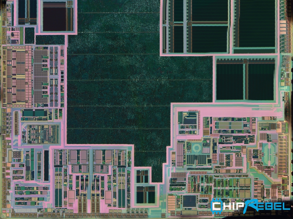
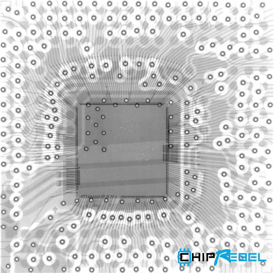
Preliminary to decapsulation the complete chip is analyzed by X-ray to give information about the location of the die and bondwires. Based on the contrast it can be said the bondwires are made of gold. As is seen in the image above the die is encapsulated in a BGA package. After decapsulation using nitric fuming acid we can have closer look at the die. The die is located a little off center as also was confirmed by the X-ray image below.

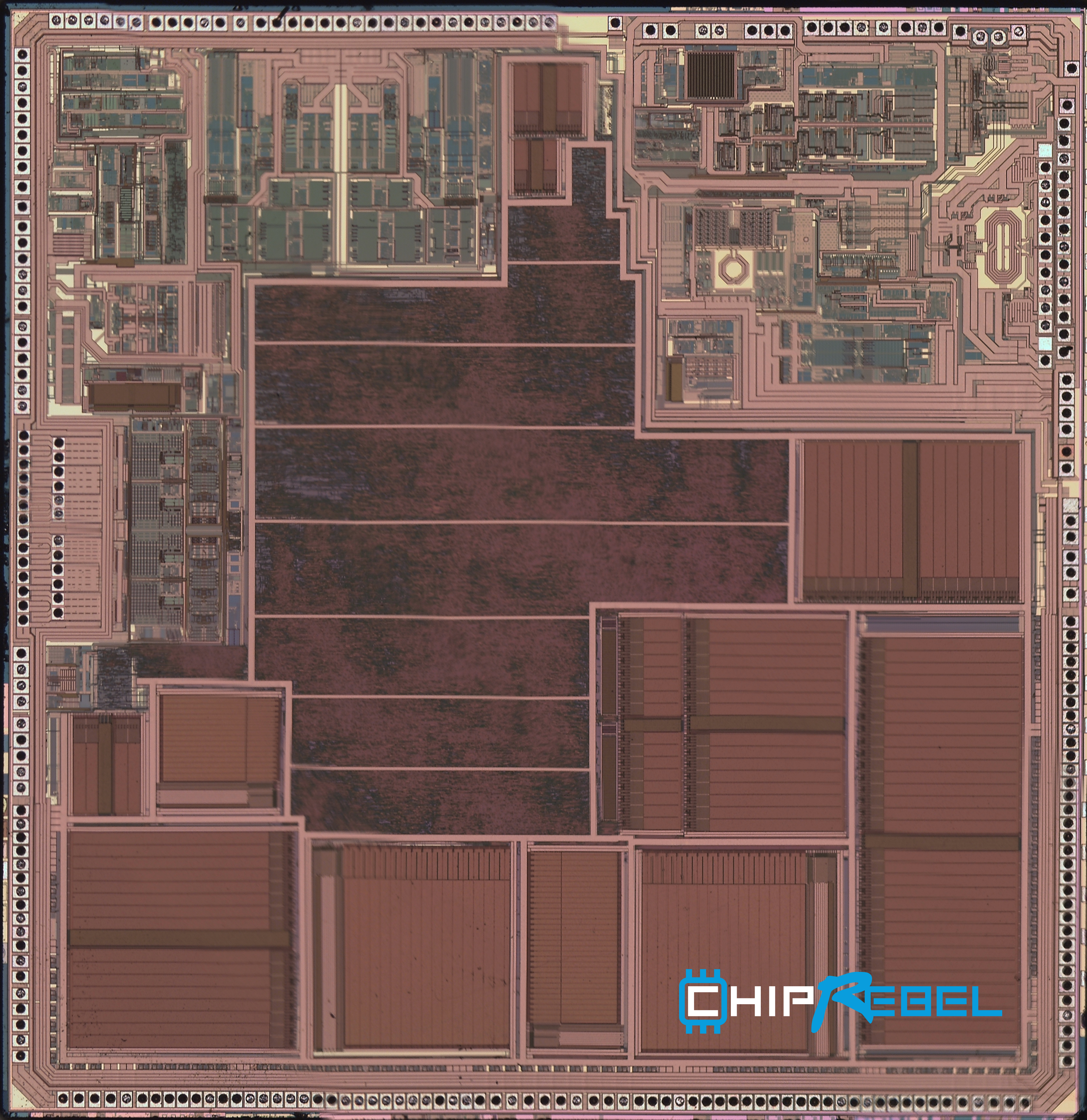

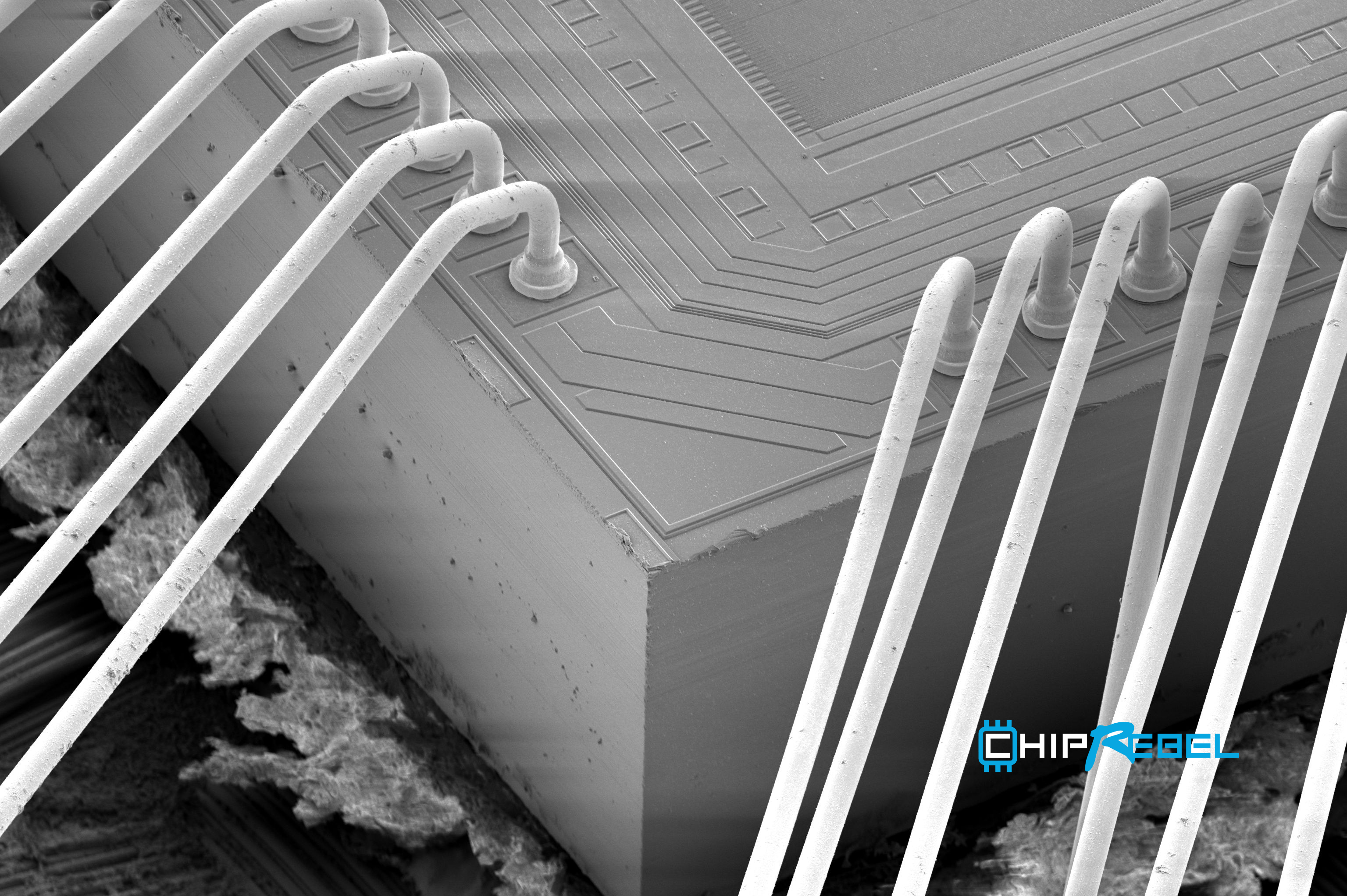
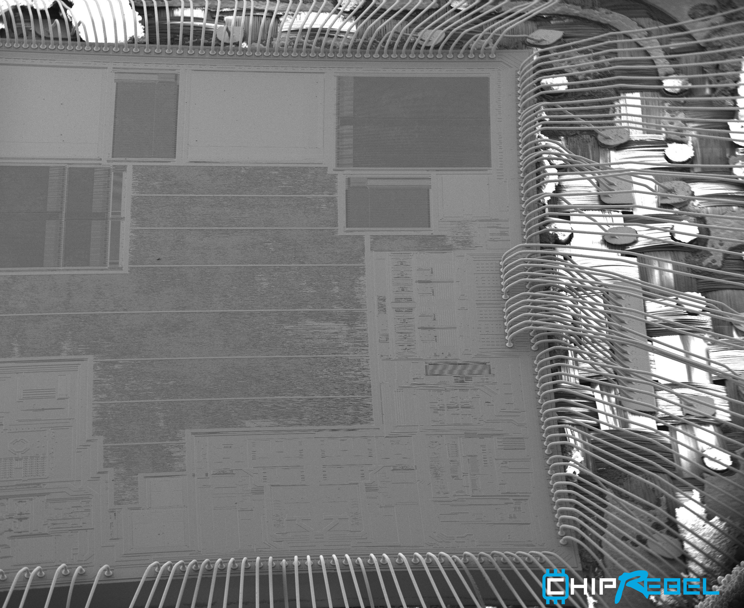
After optical microscopy we wil have an even more closer look using Scanning Electron Microscopy SEM. This way we obtain higher magnitude and more depth of focus when we use oblique view. At the left you see the unplanarized passivation of the die meaning you can see the contours of the top metal although it is still cover with a silicon oxide and a silicon nitride layer. The middle SEM image shows the scribe line as a result of the die being cut out of the wafer. On the right a more overview SEM image of the die surface showing bond wire loop. You can see the bright white part surrounding the die. These are the reinforced glass fibre matrix of the BGA substrate. They are charging in the SEM because they are insulating.
Backside Analysis
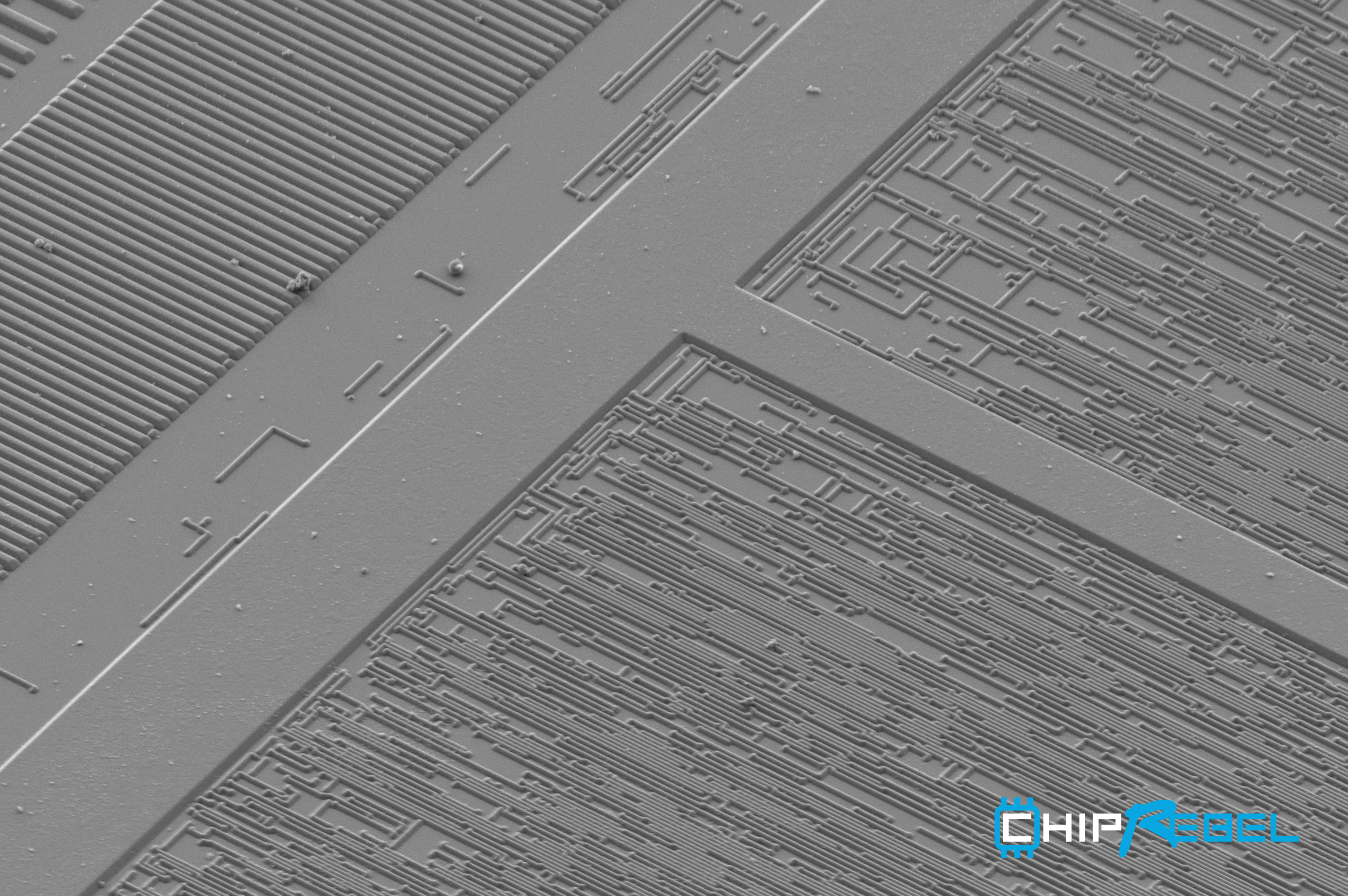
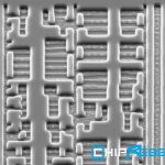
Last step is to remove all the bulk silicon of the die to obtain a clear sight on the backside. Here we will find Shallow Trench Isolation STI and gate oxide structures.


Final step is cross sectioning. We use Focussed Ion Beam FIB technique to obtain a very site specific cross section location. Another advantages of FIB is that is relatively quick, we can obtain SEM images at the same time and the cross section is polished without any mechanical deformation.
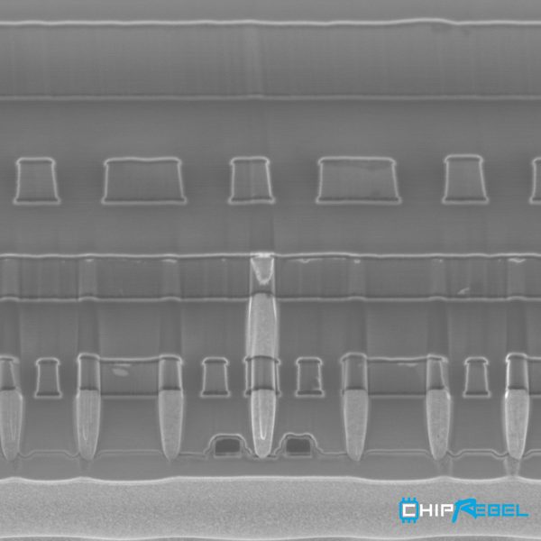
FIB cross section showing 4 aluminum metal lines, Tungsten plugs and a 250nm polysilicon physical gate length.