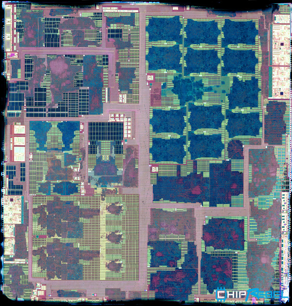
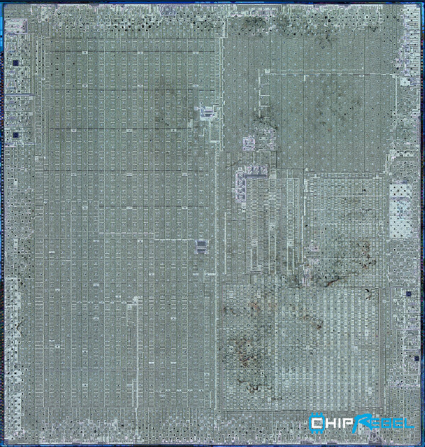
Samsung has presented the Exynos 9820 Application Processor based on Samsung’s own 8nm LPP FinFET process. This is the successor of the Exynos 9810 based on 10 nm proces node. It is used in new Samsung Galaxy smartphones like the S10e, S10, S10+ and S10 5G. See here our teardown article of the Galaxy S10.
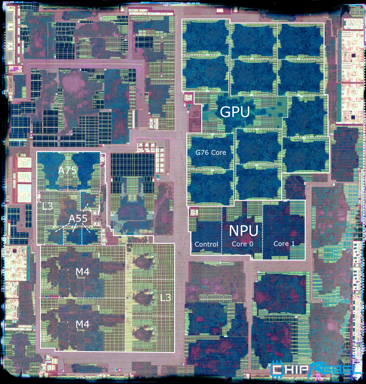
The Exynos 9820 will have a 2+2+4 core CPU configuration based on 2x Cortex A75, 4x Cortex A55 and 2x fourth generation Samsung cores (M4) as the top performing units. Furthermore a new Mali G76MP12 GPU is used and a brand new NPU is integrated. There’s a slight increase in die size. With a size of 10962 x 11581 um (sealring to sealring) we get an area of 127 mm². This is bigger than it’s predecessor the 9810 with 122 mm²
For more specifications about Samsung Exynos 9820 SoC have a look at this Anandtech article
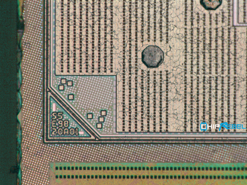
The frontside die shot of the Exynos 9820 below shows S5E9820A01 as die marking.
These images are free to use if you link us. Please respect our copyright. High resolution floorpan images can be purchased here. This article is still progress and updated frequently.