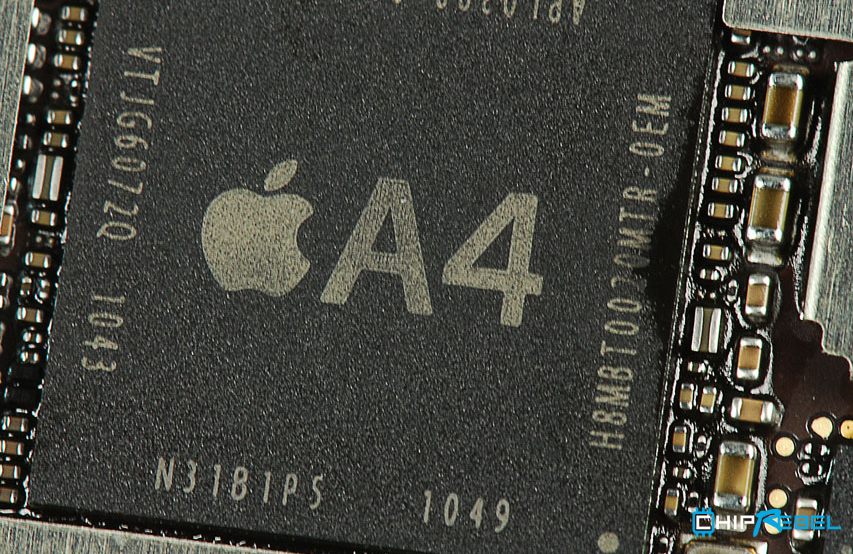
Apple’s first in-house System on chip SoC combines an ARM Cortex A8 CPU and PowerVR SGX GPU. It has been used in the first iPad and iPhone 4 and later on was substituted by the next generations A5, A6, etc. The ARM cpu has a maximum clock speed of 1GHz but besides that it has the 200MHz PowerVR SGX535 GPU onboard to do much of the graphical work. Go to the download floorplan and die utilization report section right away
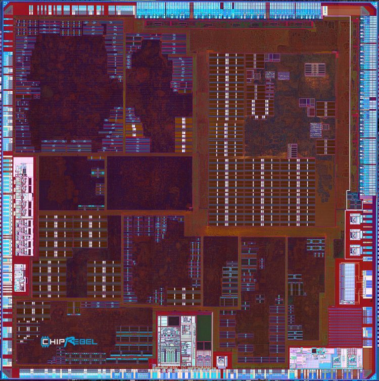
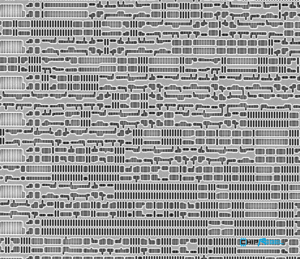
Apple’s A4 frontside optical view
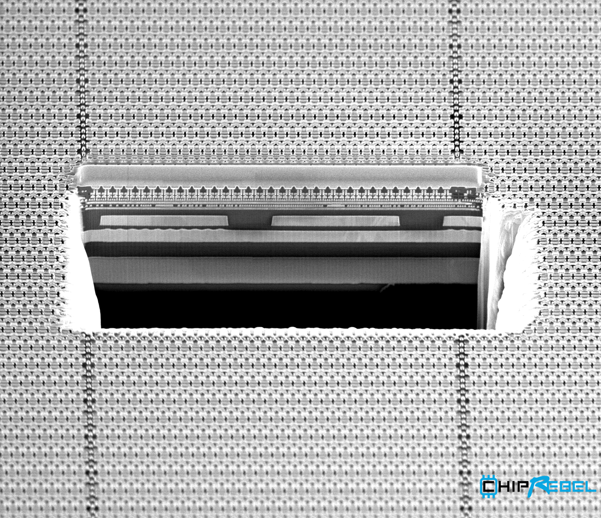
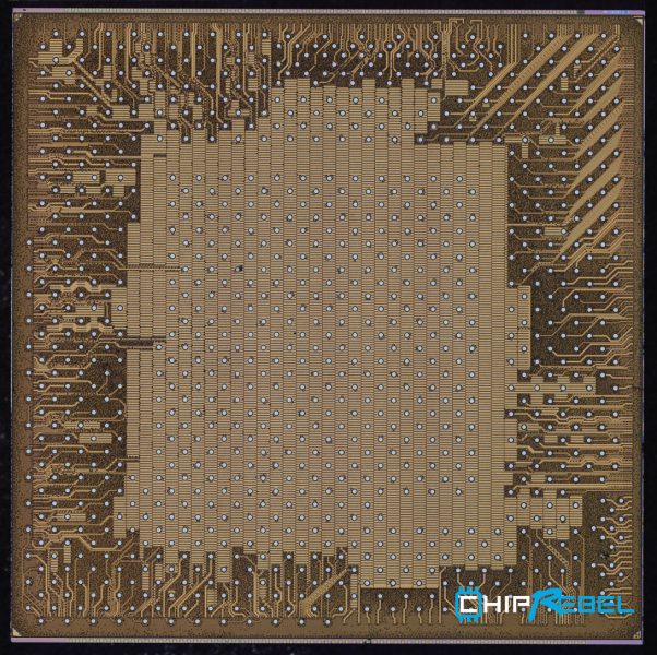
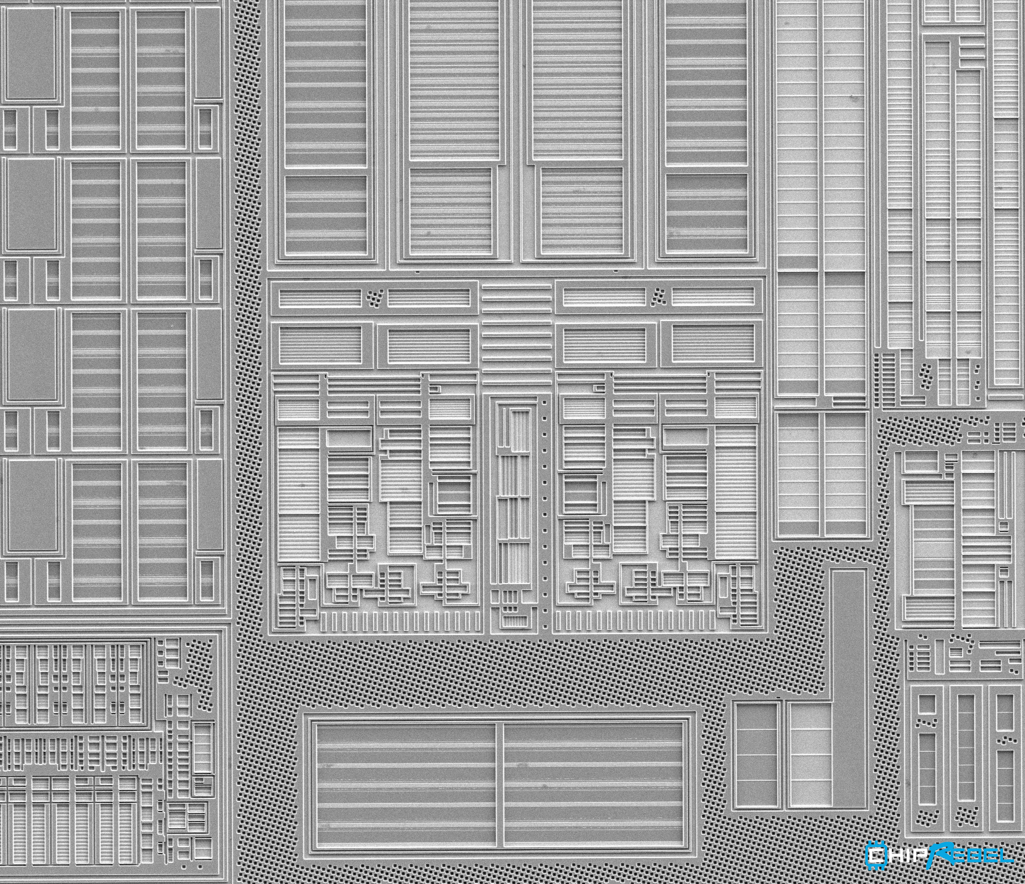
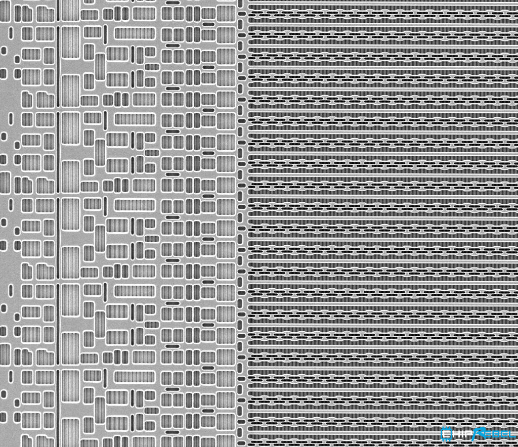
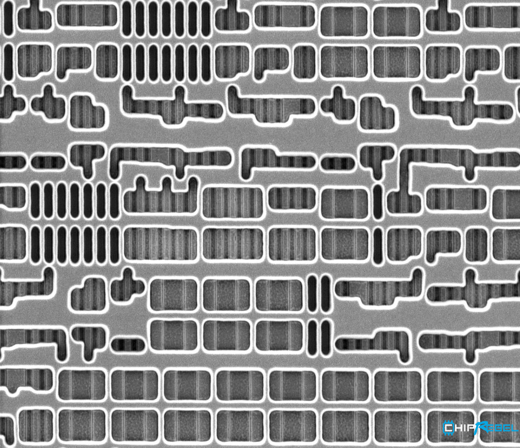
As frontside view is completely covered by the metal lines (Back-End-Of-Line, BEOL) we have removed all the bulk silicon of the die to get a clear backside view on the gate oxide and STI (silicon trench isolation). Below are some Optical Microscopy as well as SEM (Scanning Electron Microscopy) images shown.
Apple’s A4 chip backside overview
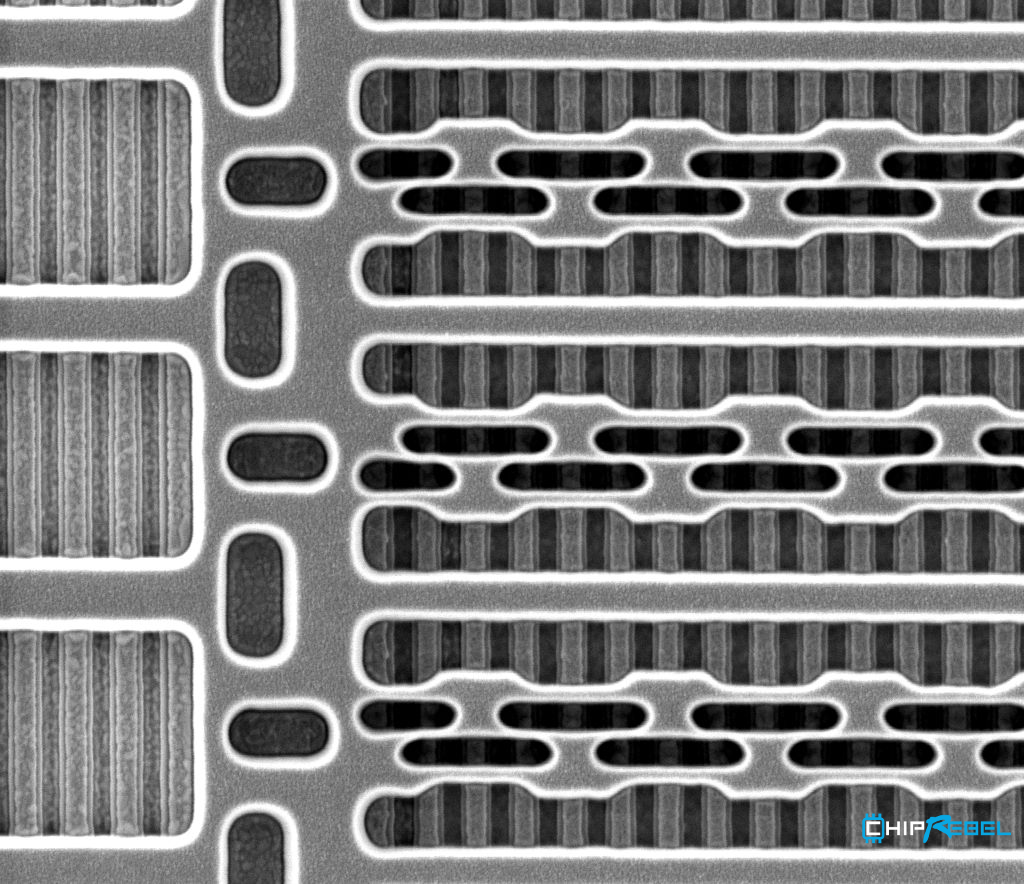
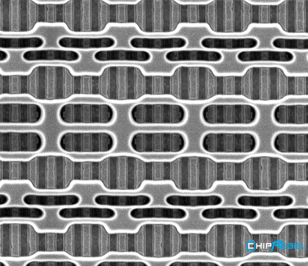
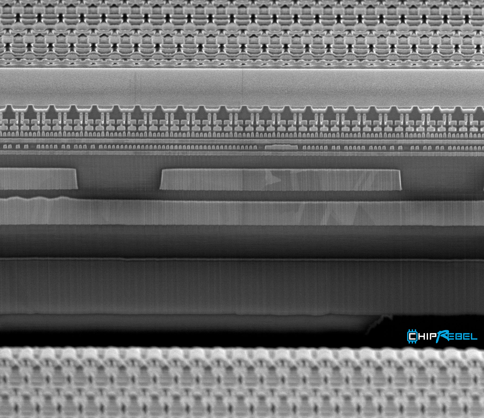
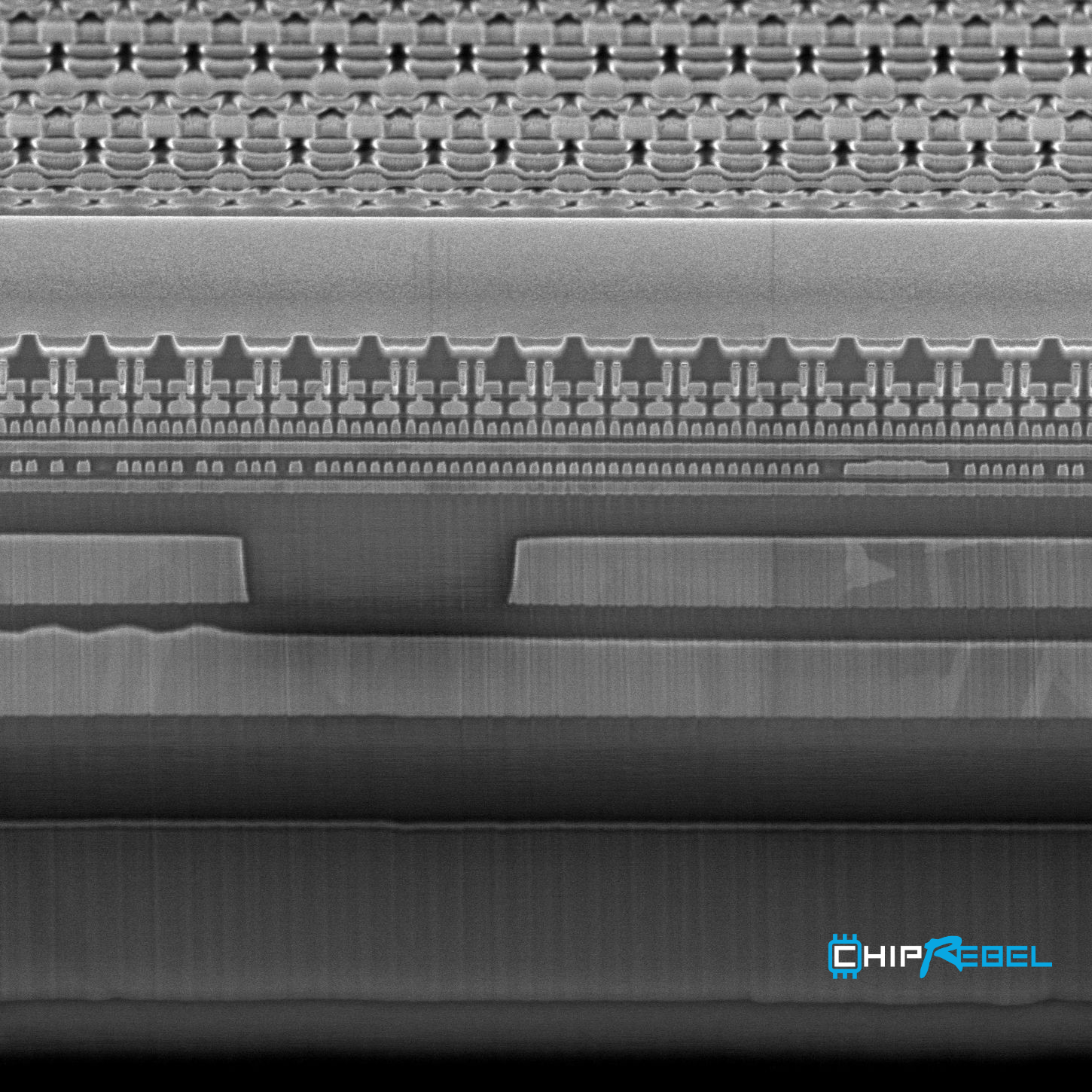
Furthermore we have made FIB cross sections to reveal it’s node technology. Physical gate length of the polysilicon gate is 65 nm. 8 copper metal lines and on top 1 aluminum AP layer is observed.