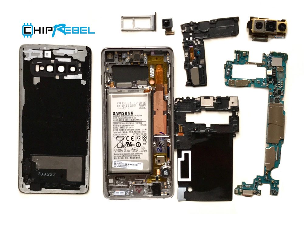
We have received Samsung’s new flagship smartphone the Galaxy S10 the day it officially is released in Europe. As mentioned here it involves two versions of the galaxy S10. North & Latin Americas, China, Japan have a version containing the Qualcomm’s Snapdragon 855 application processor. Europe & rest of the world will have a version containing Samsung’s own Exynos 9820 AP. For comparison between these two SoC’s have a look at this article.
The phone we received is the Samsung Galaxy S10 SM-G973F/DS. As mentioned we are dealing with the Exynos 9820 version which is the successor of Samsung’s Exynos 9810. For all the specifications regarding the Exynos 9820 we refer to this Anandtech article.
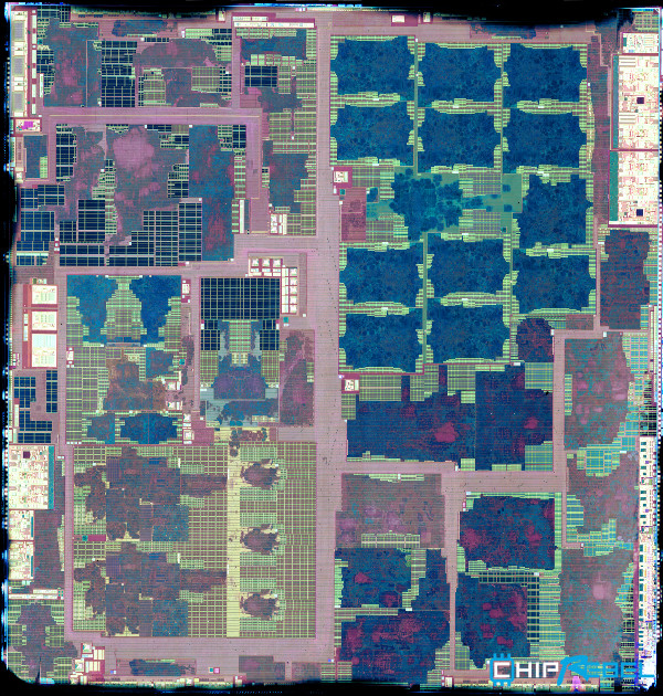
Die shot of the Samsung Exynos 9820 (click on the image to go to the article)
We have investigated the Exynos 9820 and have some magnificent die shots available here. Please be aware that our goal is to reveal the Exynos 9820 SoC and NOT producing a repair guide.
Inside the Galaxy S10 we found a motherboard (see below). Samsung itself is the prominent IC supplier, but of course they have help from other vendors. Broadcom is onboard with its BCM47752K0BIG GNSS receiver. Cirrus Logic with the CS35L40 Audio Amplifier is present two times. Murata is there with a couple of switches. NFC control is arranged by Samsung’s own SEN82LBXS2.
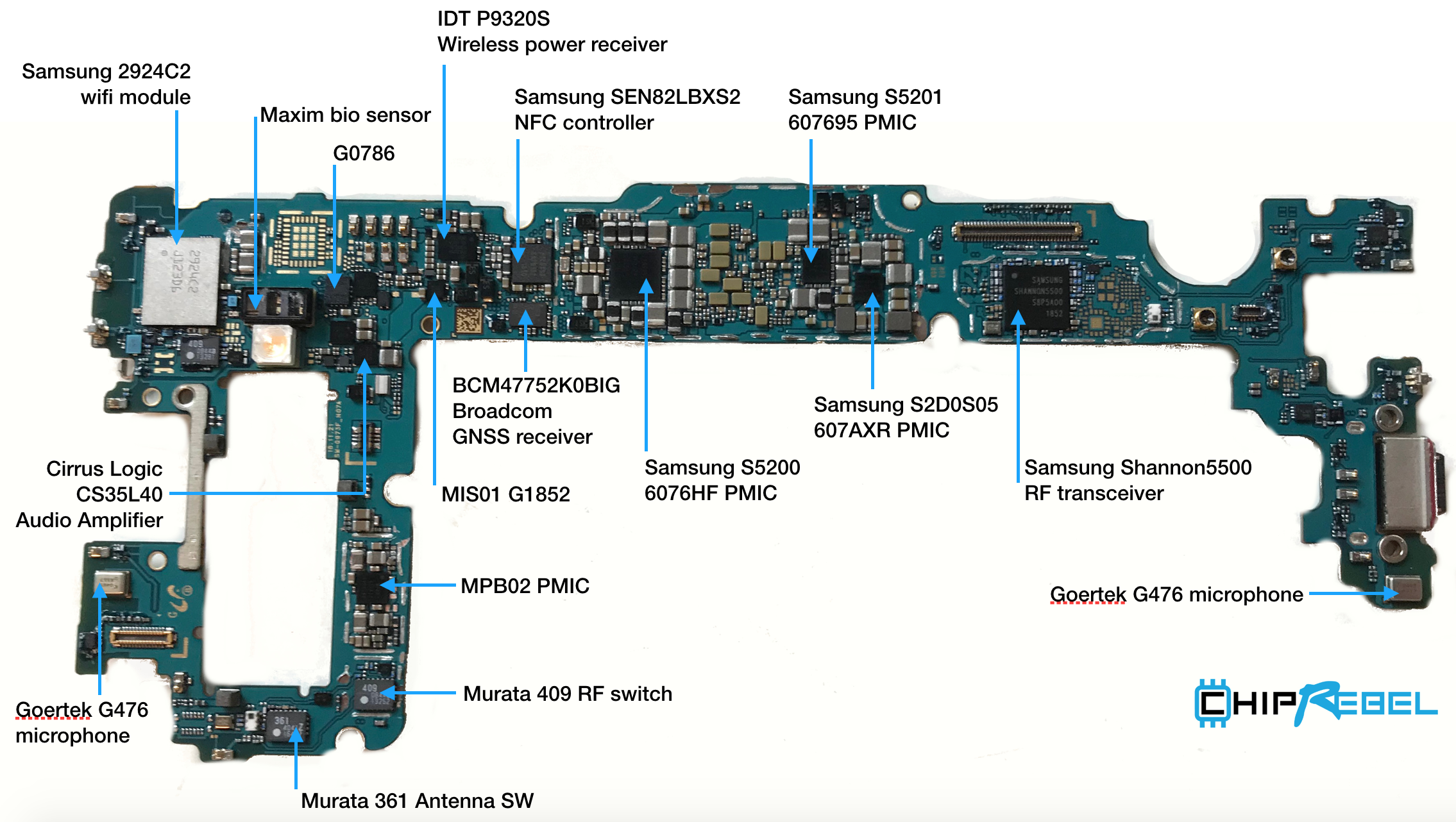
Motherboard of the Samsung Galaxy S10 frontside
We found six Power Management ICs (PMIC): Samsung Shannon 5200, Shannon 5201, Maxim MAX77705C, Samsung MPB02, Samsung MPB03 are used for the camera’s. Samsung S2DOS05 is used for the Display.
A closer look at the backside of the motherboard gives the following details. A device marked SEC 901 K3UH7H7 0MMAGCL is the Package-on-Package (PoP) containing the 8GB LPDDR4x SDRAM memory on top of the Exynos 9820 application processor (AP). This memory is Samsung’s 2nd generation 10nm-class (1y) LPDDR4X.
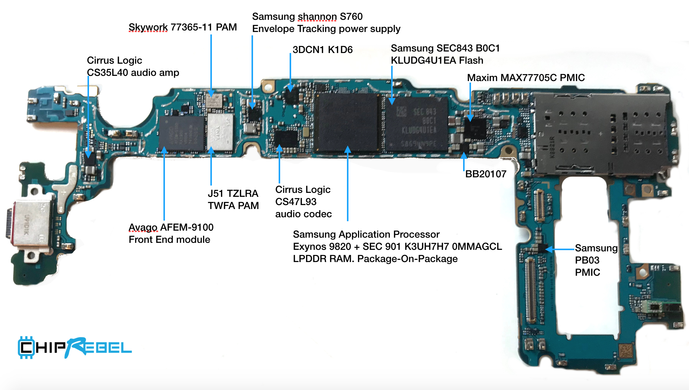
Backside view of the Samsung Galaxy S10 motherboard
Just beside the PoP Exynos 9820 SoC a chip marked SEC 843 KLUDG4U1EA-B0C1 is located. This is the 128GB UFS 2.1 flash memory
The modem inside the Exynos 9820 is said to achieve 2G/3G/4G LTE Cat 20 download speeds of 2 Gbps, (and Cat 13 upload speeds of 316 Mbps). To support the Exynos modem we find the new Samsung Shannon 5500 RF Transceiver inside the Galaxy S10.
We found six Power Management ICs (PMIC): Samsung Shannon 5200, Shannon 5201, Maxim MAX77705C, Samsung MPB02, Samsung MPB03 are used for the camera’s. Samsung S2DOS05 is used for the Display.
These images are free to use if you link to us or use credentials. Please respect our copyright. High resolution floorpan image of the Exynos can be purchased soon. This article is still in progress and will be updated during the next week…stay tuned.
In case you have questions or requests feel free to ask